


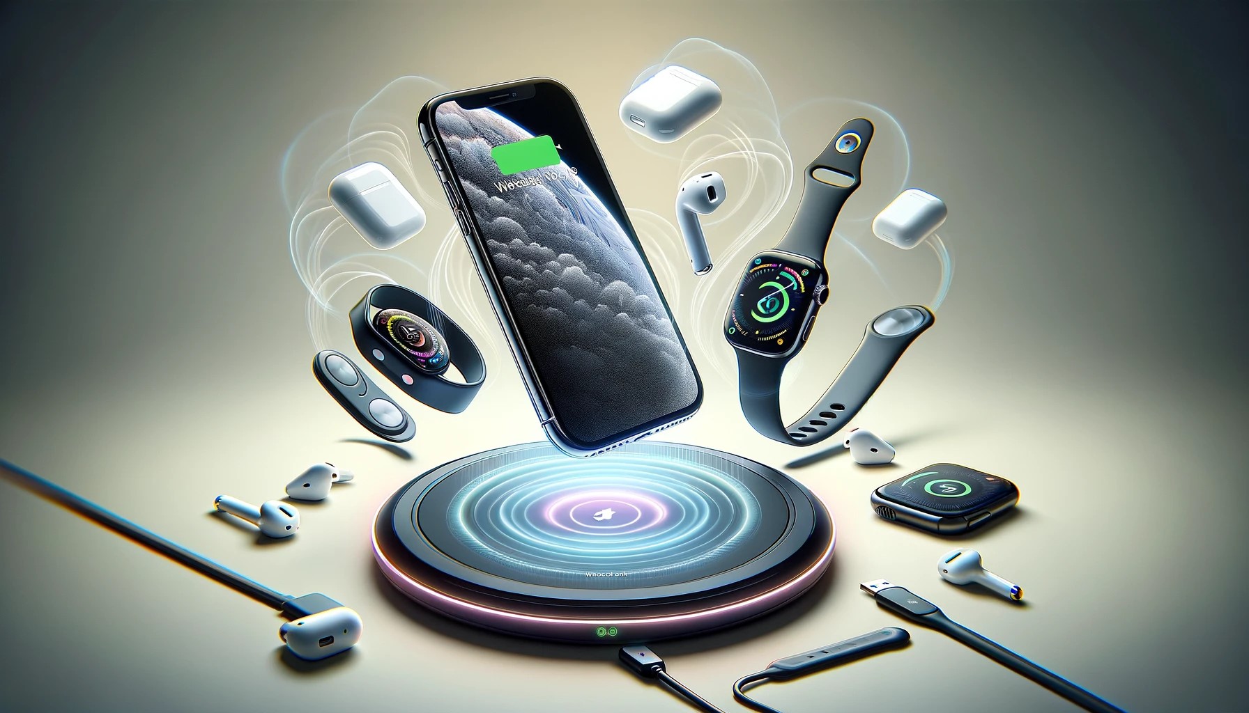
Wireless ging
Inductive ging (called wireless ging or cordless ging) uses electromagnetic fields to transfer energy between two objects through electromagnetic coupling. Energy is sent to an electrical device through an inductive coupling, which applies energy to ge the battery or run the device.应用框图
With the release of WPC Qi 2.0, many wireless ging solution providers and related industries have been concerned about Qi 2.0 certification. The release of Qi 2.0 injects fresh vitality and vitality into wireless ging, bringing countless opportunities and challenges. The convenience and safety of wireless ging are being recognized by users, and the market demand for wireless ging is also growing.
1. Principles and Development of Solutions
What is wireless ging?
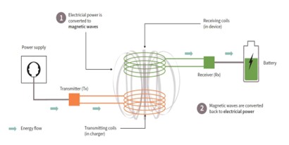
Wireless ging, simply put, is a technology that does not require the use of conductive wires. It utilizes electromagnetic induction principles, electromagnetic wave resonance principles, or other technologies that use magnetic fields as power transmission bridges. Corresponding devices are used at the transmitter and receiver ends to send and receive the generated AC signals, thereby completing the ging process.
Wireless ging for mobile phones uses magnetic induction: the primary coil generates AC power at a certain frequency, and through electromagnetic induction, a certain current is generated in the secondary coil, thereby converting energy from transmission to the receiving end.
What‘s QI2.0
As long as any digital device has the Qi logo, it means it can be ged with a Qi wireless ger. Qi 2.0 is an upgraded version of Qi, which is a comprehensive enhanced wireless ging standard developed by the WPC Wireless Charging Alliance. The ging power of Qi 2.0 has been increased from 7.5W in Qi 1.3 to 15W in Qi 2.0. At the same time, the existing BPP and EPP protocols have been optimized, forming a new MPP protocol to provide better compatibility and higher ging efficiency.
High-Performance PMIC Solution
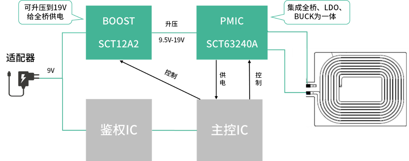
The following diagram illustrates Xinzhou Technology's transmitter solution based on MPP. The adapter provides a voltage of 9V, which is boosted to 9.5-19V by the SCT12A2 to power the full bridge. After authentication by the authentication IC and handshaking between the MCU and the receiving end, the MCU controls the full bridge to generate alternating current on the coil, causing the magnetic field on the coil to change, thereby achieving electromagnetic conversion and realizing wireless ging.
Figure 3 MPP Transmitter Scheme Diagram
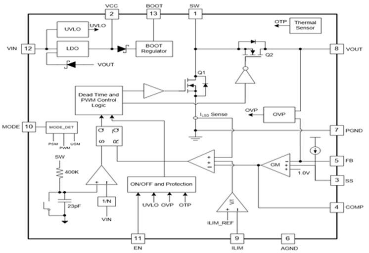
SCT12A2: This is a boost IC. In the Qi 2.0 standard, the maximum ging power is 15W. To improve efficiency, the voltage needs to be increased to reduce the current. In the Qi 2.0 standard, the maximum voltage can reach 19V. This requires a boost chip to boost the output of the adapter after the adapter, providing power to the full bridge.
SCT63240A: One channel of the full bridge generates alternating current on the coil under the control of the MCU, causing the magnetic field on the coil to change and achieve electromagnetic conversion. Another channel of LDO can provide power to the MCU. Additionally, there is a buck channel that can supply power to low-power wireless ging devices in multi-ging scenarios, such as wireless ging for watches.
Authentication IC: The authentication IC is actually a type of security chip, which serves to authenticate anti-counterfeiting, communication protection, and protect data security. It provides security protection for high-power ging. According to the requirements of the WPC's Qi 2.0 release, authentication must be included to pass the Qi 2.0 certification.
MCU: It communicates with the receiving end, regulates the output voltage of the BOOST chip, and controls the output power of the full bridge by controlling the duty cycle to adapt to the ging needs of the receiving end.
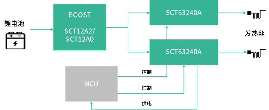
Figure 4: Electronic Cigarette Solution Diagram
Additionally, this PMIC product can also be used for highly integrated electronic cigarette solutions. Figure 4 illustrates the heating solution for electronic cigarettes. In this setup, the lithium battery voltage is supplied to the full bridge via a boost chip, and the MCU controls the full bridge to output varying power to heat the heating wire. The design and use of PMIC in this scenario share similarities with wireless ging solutions.
Introduction to Chipshow Technology Products
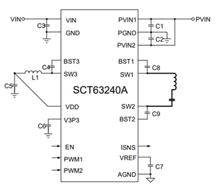
1.PMIC Solution - SCT63240A
The SCT63240A integrates full bridge, LDO, and BUCK functionalities. With a full bridge withstand voltage of 20V and a power output of 20W, it integrates a 3.3V/200mA LDO and a 5V/1A BUCK. No additional LDO is required to supply power to the MCU, greatly simplifying the TX schematic diagram and reducing the cost and materials of the solution.
· VIN Input Voltage Range: 4.2V-20V
· PVIN Input Voltage Range: 1V~17V
· Up to 20W Power Transfer
· Integrated Full-Bridge Power Stage with 14.5- mΩ Rdson of Power MOSFETs
· Integrated High Efficiency 5V-1A Step-down DC/DC Converter
· Optimized for EMI Reduction
· Build-in 3.3V-200mA LDO
· Provide 2.5V Voltage Reference
· Integrated Lossless Input Current Sensor with ±2% accuracy for FOD and current Demodulation
· 3.3V and 5V PWM Signal Logic Compatible
· Input Under-Voltage Lockout
· Over Current Protection
· Over Temperature Protection
· 3mm*4mm QFN-19L Package
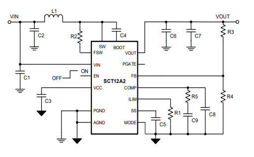
2.BOOST Solution - SCT12A2
The SCT12A2 is a boost IC with a maximum output voltage of 21V, switch current of 15A, and output power of over 30W, fully meeting the requirements of Qi 2.0. It can drive a P-MOSFET as a load switch, solving the problem of BOOST IC not being able to completely turn off.
3.BOOST Upgrade Solution - SCT12A5
In the MPP solution, two points that customers are particularly concerned about are efficiency and size. The SCT12A5 has been greatly optimized in both aspects:
* Efficiency: Under the conditions of input 9V and output 17V with a power of 21W, the efficiency reaches 97%.
* Size: With a smaller package size, the QFN3*4 dimensions meet smaller space requirements.


 京公网安备 11010802042628号